Buku Persamaan Ic Dan Transistor Amplifier
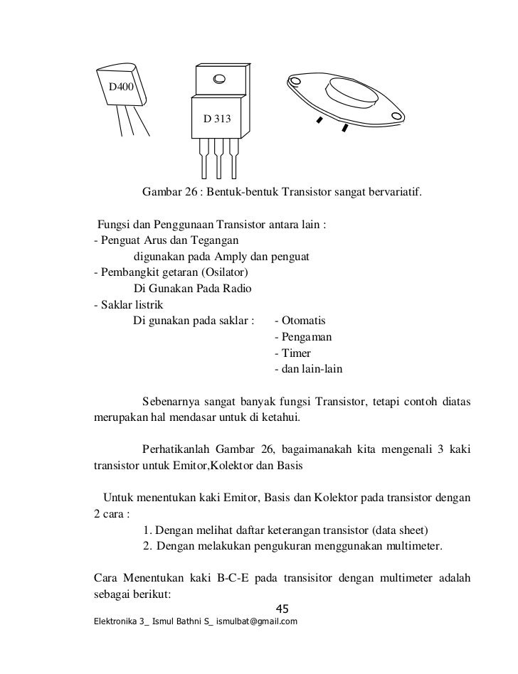
Transistor dalam rangkaian elektronik berfungsi antara lain sebagai penguat (amplifier), oscillator, converter tegangan DC, loading-driver (pengemudi beban), phase-shifter (perubah fasa), dan lain-lain. Transistor bipolar adalah transistor yang paling banyak dan.
Type Designator: 2N5551
Material of Transistor: Si
Polarity: NPN
Maximum Collector Power Dissipation (Pc): 0.31 W
Maximum Collector-Base Voltage Vcb : 180 V
Maximum Collector-Emitter Voltage Vce : 160 V
Maximum Emitter-Base Voltage Veb : 6 V
Maximum Collector Current Ic max : 0.6 A
Max. Operating Junction Temperature (Tj): 135 °C
Transition Frequency (ft): 100 MHz
Collector Capacitance (Cc): 6 pF
Forward Current Transfer Ratio (hFE), MIN: 80
Noise Figure, dB: -
This is can be used for example to use WiiGator’s 0.2 GC backup launcher instead of the modified version NeoGamma usesinternal.:Launches the included GC backup launcher, which is a modification of WiiGator’s 0.2 GC backup launcher. Cmios rev 3 installer download.
Package: TO92
2N5551 Transistor Equivalent Substitute - Cross-Reference Search
2N5551 Datasheet (PDF)
1.1. 2n5551g.pdf Size:189K _upd
UNISONIC TECHNOLOGIES CO., LTD 2N5551 NPN SILICON TRANSISTOR HIGH VOLTAGE SWITCHING TRANSISTOR FEATURES * High collector-emitter voltage: VCEO=160V * High current gain APPLICATIONS * Telephone switching circuit * Amplifier ORDERING INFORMATION Ordering Number Pin Assignment Package Packing Lead Free Plating Halogen Free 1 2 3 2N5551L-x-AB3-R 2N5551G-x-
1.2. 2n5551sc.pdf Size:339K _upd
SEMICONDUCTOR 2N5551SC TECHNICAL DATA EPITAXIAL PLANAR NPN TRANSISTOR GENERAL PURPOSE APPLICATION. HIGH VOLTAGE APPLICATION. E L B L FEATURES ·High Collector Breakdwon Voltage DIM MILLIMETERS _ + A 2.90 0.1 2 3 : VCBO=180V, VCEO=160V B 1.30+0.20/-0.15 C 1.30 MAX ·Low Leakage Current. 1 D 0.40+0.15/-0.05 : ICBO=50nA(Max.) VCB=120V E 2.40+0.30/-0.20 G 1.90 ·Low Saturatio
1.3. 2n5551csm.pdf Size:31K _upd
2N5551CSM HIGH VOLTAGE NPN SWITCHING TRANSISTOR IN A HERMETICALLY SEALED MECHANICAL DATA CERAMIC SURFACE MOUNT PACKAGE Dimensions in mm (inches) FOR HIGH RELIABILITY APPLICATIONS 0.51 ± 0.10 (0.02 ± 0.004) 0.31 FEATURES rad. (0.012) • SILICON PLANAR EPITAXIAL NPN 3 TRANSISTOR • HERMETIC CERAMIC SURFACE MOUNT PACKAGE (SOT23 COMPATIBLE) 21 • CECC SCREENING OPTIONS 1.9
1.4. 2n5551k.pdf Size:550K _upd
Typical Characterisitics 2N5551K hFE —— IC Static Characteristic 50 1000 COMMON EMITTER 300uA Ta=25℃ 270uA 40 Ta=100℃ 240uA 210uA 30 180uA 100 Ta=25℃ 150uA 20 120uA 90uA 10 60uA COMMON EMITTER IB=30uA VCE=5V 0 10 02468 110 100 200 COLLECTOR-EMITTER VOLTAGE VCE (V) COLLECTOR CURRENT IC (mA) VCEsat —— IC VBEsat —— IC 1000 2 1 Ta=25℃ Ta=10
1.5. 2n5551hr.pdf Size:428K _upd
2N5551HR Hi-Rel NPN bipolar transistor 160 V, 0.5 A Datasheet - production data Features 3 BVCEO 160 V 1 1 IC (max) 0.5 A 2 2 3 HFE at 5 V - 10 mA > 80 TO-18 LCC-3 3 • Hermetic packages 4 • ESCC and JANS qualified 1 • Up to 100 krad(Si) low dose rate 2 UB Description Pin 4 in UB is connected to the metallic lid. The 2N5551HR is a silicon planar NPN transistor spe
1.6. 2n5551dcsm.pdf Size:10K _upd
2N5551DCSM Dimensions in mm (inches). Dual Bipolar NPN Devices in a hermetically sealed LCC2 Ceramic Surface Mount Package for High Reliability 1.40 ± 0.15 2.29 ± 0.20 1.65 ± 0.13 (0.055 ± 0.006) (0.09 ± 0.008) (0.065 ± 0.005) Applications 2 3 1 4 Dual Bipolar NPN Devices. A 0.23 6 5 rad. (0.009) V = 160V CEO 6.22 ± 0.13 A = 1.27 ± 0.13 I = 0.6A C (0.
1.7. 2n5551cn.pdf Size:249K _upd
2N5551CN Semiconductor Semiconductor NPN Silicon Transistor Descriptions • General purpose amplifier • High voltage application Features • High collector breakdown voltage : VCBO = 180V, VCEO = 160V • Low collector saturation voltage : VCE(sat)=0.5V(MAX.) Ordering Information Type NO. Marking Package Code 2N5551CN 2N5551C TO-92N Outline Dimensions unit : mm 4.20
1.8. 2n5551n.pdf Size:249K _upd
2N5551N Semiconductor Semiconductor NPN Silicon Transistor Descriptions • General purpose amplifier • High voltage application Features • High collector breakdown voltage : VCBO = 180V, VCEO = 160V • Low collector saturation voltage : VCE(sat)=0.5V(MAX.) • Complementary pair with 2N5401N Ordering Information Type NO. Marking Package Code 2N5551N 2N5551 TO-9
1.9. 2n5550 2n5551.pdf Size:188K _motorola
MOTOROLA Order this document SEMICONDUCTOR TECHNICAL DATA by 2N5550/D Amplifier Transistors 2N5550 NPN Silicon * 2N5551 *Motorola Preferred Device COLLECTOR 3 2 BASE 1 EMITTER 1 2 3 MAXIMUM RATINGS Rating Symbol 2N5550 2N5551 Unit CASE 29–04, STYLE 1 TO–92 (TO–226AA) Collector–Emitter Voltage VCEO 140 160 Vdc Collector–Base Voltage VCBO 160 180 Vdc Emitter–Base Voltage VEB
1.10. 2n5550 2n5551 3.pdf Size:49K _philips
DISCRETE SEMICONDUCTORS DATA SHEET book, halfpage M3D186 2N5550; 2N5551 NPN high-voltage transistors 1999 Apr 23 Product specification Supersedes data of 1997 Apr 09 Philips Semiconductors Product specification NPN high-voltage transistors 2N5550; 2N5551 FEATURES PINNING • Low current (max. 300 mA) PIN DESCRIPTION • High voltage (max. 160 V). 1 collector 2 base APPLICATIONS 3 em
1.11. 2n5550 2n5551 2.pdf Size:53K _philips
DISCRETE SEMICONDUCTORS DATA SHEET book, halfpage M3D186 2N5550; 2N5551 NPN high-voltage transistors Product specification 2004 Oct 28 Supersedes data of 1999 Apr 23 Philips Semiconductors Product specification NPN high-voltage transistors 2N5550; 2N5551 FEATURES PINNING • Low current (max. 300 mA) PIN DESCRIPTION • High voltage (max. 160 V). 1 collector 2 base APPLICATIONS 3 emi
1.12. 2n5551.pdf Size:216K _fairchild_semi
April 2006 2N5551- MMBT5551 tm NPN General Purpose Amplifier Features • This device is designed for general purpose high voltage amplifiers and gas discharge display drivers. • Suffix “-C” means Center Collector in 2N5551 (1. Emitter 2. Collector 3. Base) • Suffix “-Y” means hFE 180~240 in 2N5551 (Test condition : IC = 10mA, VCE = 5.0V) 2N5551 MMBT5551 3 2 TO-92 SOT-23 1 Marking: 3S
1.13. 2n5551 mmbt5551.pdf Size:171K _fairchild_semi
June 2009 2N5551 / MMBT5551 NPN General Purpose Amplifier Features • This device is designed for general purpose high voltage amplifiers and gas discharge display drivers. • Suffix “-C” means Center Collector in 2N5551 (1. Emitter 2. Collector 3. Base) • Suffix “-Y” means hFE 180~240 in 2N5551 (Test condition : IC = 10mA, VCE = 5.0V) 2N5551 MMBT5551 3 2 TO-92 SOT-23 1 Marking: 3S
1.14. 2n5551.pdf Size:53K _samsung
2N5551 NPN EPITAXIAL SILICON TRANSISTOR AMPLIFIER TRANSISTOR • Collector-Emitter Voltage: VCEO= 160V TO-92 • Collector Dissipation: PC (max)=625mW ABSOLUTE MAXIMUM RATINGS (T =25 ) A Characteristic Symbol Rating Unit Collector-Base Voltage VCBO 180 V Collector-Emitter Voltage VCEO 160 V Emitter-Base Voltage VEBO 6 V Collector Current IC 600 mA Collector Dissipation PC 625 mW Junction
1.15. 2n5550 2n5551.pdf Size:64K _central
145 Adams Avenue, Hauppauge, NY 11788 USA Tel: (631) 435-1110 • Fax: (631) 435-1824
1.16. 2n5551 to-92.pdf Size:208K _mcc
MCC Micro Commercial Components TM 2N5551 20736 Marilla Street Chatsworth Micro Commercial Components CA 91311 Phone: (818) 701-4933 Fax: (818) 701-4939 Features • This device is designed for general purpose high voltage amplifiers NPN General and gas discharge display drivers. Purpose Amplifier • Epoxy meets UL 94 V-0 flammability rating • Moisure Sensitivity Level 1 Transistor
1.17. 2n5550 2n5551.pdf Size:88K _onsemi
2N5550, 2N5551 Preferred Device Amplifier Transistors NPN Silicon Features • These are Pb-Free Devices* http://onsemi.com COLLECTOR 3 MAXIMUM RATINGS 2 Rating Symbol Value Unit BASE Collector - Emitter Voltage VCEO Vdc 2N5550 140 1 2N5551 160 EMITTER Collector - Base Voltage VCBO Vdc 2N5550 160 2N5551 180 Emitter - Base Voltage VEBO 6.0 Vdc TO-92 CASE 29 Collector Current -
1.18. 2n5551.pdf Size:178K _utc
UNISONIC TECHNOLOGIES CO., LTD 2N5551 NPN SILICON TRANSISTOR HIGH VOLTAGE SWITCHING TRANSISTOR ? FEATURES * High collector-emitter voltage: VCEO=160V * High current gain ? APPLICATIONS * Telephone switching circuit * Amplifier ? ORDERING INFORMATION Ordering Number Pin Assignment Package Packing Lead Free Plating Halogen Free 1 2 3 2N5551L-x-AB3-R 2N5551G-x-AB3-R SOT
1.19. 2n5551.pdf Size:217K _auk
2N5551 NPN Silicon Transistor Descriptions PIN Connection • General purpose amplifier C • High voltage application Features B • High collector breakdown voltage : VCBO = 180V, VCEO = 160V • Low collector saturation voltage : E VCE(sat)=0.5V(MAX.) TO-92 • Complementary pair with 2N5401 Ordering Information Type NO. Marking Package Code 2N5551 2N5551 TO
1.20. 2n5551.pdf Size:203K _secos
2N5551 NPN Silicon Elektronische Bauelemente General Purpose Transistor RoHS Compliant Product A suffix of '-C' specifies halogen & lead-free TO-92 4.55±0.2 3.5±0.2 FEATURES * Switching and amplification in high voltage * Low current(max. 600mA) * High voltage(max.180v) 0.43+0.08 –0.07 46+0.1 0. –0.1 (1.27 Typ.) 1: Emitter +0.2 1.25–0.2 2: Base 1 2 3 3: Collecto
1.21. 2n5551.pdf Size:279K _cdil
Continental Device India Limited An ISO/TS 16949, ISO 9001 and ISO 14001 Certified Company NPN EPITAXIAL PLANAR SILICON HIGH VOLTAGE TRANSISTOR 2N5551 TO- 92 CBE C B E High Voltage NPN Transistor For General Purpose And Telephony Applications. ABSOLUTE MAXIMUM RATINGS(Ta=25deg C unless otherwise specified) DESCRIPTION SYMBOL VALUE UNIT Collector -Emitter Voltage VCEO 160 V Collector -B
1.22. 2n5551s.pdf Size:33K _kec
SEMICONDUCTOR 2N5551S TECHNICAL DATA EPITAXIAL PLANAR NPN TRANSISTOR GENERAL PURPOSE APPLICATION. HIGH VOLTAGE APPLICATION. E L B L DIM MILLIMETERS FEATURES _ + 2.93 0.20 A B 1.30+0.20/-0.15 High Collector Breakdwon Voltage C 1.30 MAX 2 : VCBO=180V, VCEO=160V 3 D 0.45+0.15/-0.05 E 2.40+0.30/-0.20 Low Leakage Current. 1 G 1.90 H 0.95 : ICBO=50nA(Max.) VCB=120V J 0.13+0.1
1.23. 2n5551.pdf Size:32K _kec
SEMICONDUCTOR 2N5551 TECHNICAL DATA EPITAXIAL PLANAR NPN TRANSISTOR GENERAL PURPOSE APPLICATION. HIGH VOLTAGE APPLICATION. B C FEATURES High Collector Breakdwon Voltage N DIM MILLIMETERS : VCBO=180V, VCEO=160V A 4.70 MAX E K Low Leakage Current. B 4.80 MAX G C 3.70 MAX D : ICBO=50nA(Max.), VCB=120V D 0.45 E 1.00 Low Saturation Voltage F 1.27 G 0.85 : VCE(sat)=0.2V(Max.),
1.24. 2n5551c.pdf Size:32K _kec
SEMICONDUCTOR 2N5551C TECHNICAL DATA EPITAXIAL PLANAR NPN TRANSISTOR GENERAL PURPOSE APPLICATION. HIGH VOLTAGE APPLICATION. B C FEATURES High Collector Breakdwon Voltage N DIM MILLIMETERS : VCBO=180V, VCEO=160V A 4.70 MAX E K Low Leakage Current. B 4.80 MAX G C 3.70 MAX D : ICBO=50nA(Max.), VCB=120V D 0.45 E 1.00 Low Saturation Voltage F 1.27 G 0.85 : VCE(sat)=0.2V(Max.),
1.25. 2n5551.pdf Size:220K _lge
2N5551(NPN) TO-92 Bipolar Transistors TO-92 1. EMITTER 2. BASE 3. COLLECTOR Features Switching and amplification in high voltage Applications such as telephony Low current(max. 600mA) High voltage(max.180V) MAXIMUM RATINGS (TA=25? unless otherwise noted) Dimensions in inches and (millimeters) Symbol Parameter Value Units VCBO Collector-Base Voltage 180 V VC
1.26. 2n5551.pdf Size:386K _wietron
2N5551 NPN Transistors TO-92 1. EMITTER 1 2 2. BASE 3 3. COLLECTOR ABSOLUTE MAXIMUM RATINGS (Ta=25 C) Rating Symbol 2N5551 Unit Collector-Emitter Voltage V CEO 160 Vdc Collector-Base Voltage VCBO 180 Vdc Emitter-Base VOltage VEBO 6.0 Vdc Collector Current IC 600 mAdc PD Total Device Dissipation T =25 C W A 0.625 Junction Temperature T 150 j C Storage, Temperature Tstg C
1.27. h2n5551.pdf Size:52K _hsmc
Spec. No. : HE6219 HI-SINCERITY Issued Date : 1992.09.21 Revised Date : 2004.12.28 MICROELECTRONICS CORP. Page No. : 1/5 H2N5551 NPN EPITAXIAL PLANAR TRANSISTOR Description The H2N5551 is designed for amplifier transistor. Features TO-92 • Complements to PNP Type H2N5401 • High Collector-Emitter Breakdown Voltage (VCEO>160V (@IC=1mA)) Absolute Maximum Ratings • Maximum Tempera
1.28. 2n5551.pdf Size:260K _can-sheng
TO-92 Plastic-Encapsulate Transistors TO-92 TO-92 TO-92 TO-92 TRANSISTOR (NPN) 2N5551 TRANSISTOR (NPN) TRANSISTOR (NPN) TRANSISTOR (NPN) FEATURES FEATURES FEATURES FEATURES � Switching and amplification in high voltage � Switching and amplification in high voltage � Switching and amplification in high voltage � Switching and amplification in high voltage 1. EMlTTER �
1.29. 2n5551.pdf Size:136K _first_silicon
SEMICONDUCTOR 2N5551 TECHNICAL DATA 2N5551 TRANSISTOR (NPN) B C FEATURES General Purpose Switching Application DIM MILLIMETERS A 4.70 MAX E B 4.80 MAX G C 3.70 MAX D MAXIMUM RATINGS (Ta=25℃ unless otherwise noted) D 0.55 MAX E 1.00 F 1.27 Symbol Parameter Value Unit G 0.85 H 0.45 VCBO Collector-Base Voltage 180 V _ H J 14.00 0.50 + L 2.30 F F VCEO Collector-E
1.30. 2n5551.pdf Size:1058K _shenzhen-tuofeng-semi
Shenzhen Tuofeng Semiconductor Technology Co., Ltd TO-92 Plastic-Encapsulate Transistors 2N5551 TRANSISTOR( NPN ) TO-92 FEATURES ·Switching and amplification in high voltage Applications such as telephony 1. EMITTER · Low current(max. 600mA) 2. BASE · High voltage(max.180v) 3. COLLECTOR 1 2 3 MAXIMUM RATINGS* TA=25℃ unless otherwise noted Symbol Parame
Datasheet: 2N5538, 2N5539, 2N554, 2N5540, 2N5541, 2N5542, 2N555, 2N5550, MJE13005, 2N5552, 2N5552-1, 2N5552-2, 2N5552-4, 2N5559, 2N556, 2N5560, 2N557.
LIST
Last Update
BJT: UNR221Z UNR221V UNR221T UNR221N UNR221M UNR221L UNR221K UNR221F UNR221E UNR221D UNR2219 UNR2218 UNR2217 UNR2216 UNR2215 UNR2214 UNR2213 UNR2212 UNR2211 UNR2210
Type Designator: A1015
Material of Transistor: Si
Polarity: PNP
Maximum Collector Power Dissipation (Pc): 0.2 W
Maximum Collector-Base Voltage Vcb : 50 V
Maximum Collector-Emitter Voltage Vce : 50 V
Maximum Emitter-Base Voltage Veb : 5 V
Maximum Collector Current Ic max : 0.15 A
Max. Operating Junction Temperature (Tj): 125 °C
Transition Frequency (ft): 80 MHz
Forward Current Transfer Ratio (hFE), MIN: 130
Noise Figure, dB: -
Package: SOT23
A1015 Transistor Equivalent Substitute - Cross-Reference Search
A1015 Datasheet (PDF)
1.1. 2sa1015-gr.pdf Size:504K _update
2SA1015-O MCC Micro Commercial Components TM 2SA1015-Y 20736 Marilla Street Chatsworth Micro Commercial Components CA 91311 2SA1015-GR Phone: (818) 701-4933 Fax: (818) 701-4939 Features • Capable of 0.4Watts of Power Dissipation. PNP Silicon • Collector-current 0.15A • Collector-base Voltage 50V Plastic-Encapsulate • Operating and storage junction temperature range: -
1.2. 2sa1015-y.pdf Size:504K _update
2SA1015-O MCC Micro Commercial Components TM 2SA1015-Y 20736 Marilla Street Chatsworth Micro Commercial Components CA 91311 2SA1015-GR Phone: (818) 701-4933 Fax: (818) 701-4939 Features • Capable of 0.4Watts of Power Dissipation. PNP Silicon • Collector-current 0.15A • Collector-base Voltage 50V Plastic-Encapsulate • Operating and storage junction temperature range: -
1.3. a1015s.pdf Size:263K _update
A1015S 风光欣技术资料 —PNP Silicon— PNP Transistors ■■ APPLICATION:Low Frequency Amplifier Applications. ■■ MAXIMUM RATINGS(Ta=25℃) PARAMETER SYMBOL RATING UNIT VCBO -50 V Collector-base voltage VCEO -50 V Collector-emitter voltage VEBO -5 V Emitter-base voltage IC -0.15 A Collector current PC 0.3 Collector Power Dissipation W Tj 150 ℃ Junc
1.4. 2sa1015-o.pdf Size:504K _update
2SA1015-O MCC Micro Commercial Components TM 2SA1015-Y 20736 Marilla Street Chatsworth Micro Commercial Components CA 91311 2SA1015-GR Phone: (818) 701-4933 Fax: (818) 701-4939 Features • Capable of 0.4Watts of Power Dissipation. PNP Silicon • Collector-current 0.15A • Collector-base Voltage 50V Plastic-Encapsulate • Operating and storage junction temperature range: -
1.5. 2sa1015lt1.pdf Size:145K _update
SEMICONDUCTOR 2SA1015LT1 Shandong Yiguang Electronic Joint stock Co., Ltd TECHNICAL DATA PNP EPITAXIAL SILICON TRANSISTOR Package:SOT-23 * Complement to 2SC1815 * Collector Current : Ic=150mA ABSOLUTE MAXIMUM RATINGS at Ta=25℃ Characteristic Symbol Rating Unit Collector-Base Voltage Vcbo -60 V Collector-Emitter Voltage Vceo -50 V PIN: 1 2 3 Emitter-Base Voltage Vebo -5 V
1.6. bta1015a3.pdf Size:151K _upd
Spec. No. : C306A3-T 查询'BTA1015A3'供应商 Issued Date : 2003.08.26 CYStech Electronics Corp. Revised Date : Page No. : 1/4 General Purpose PNP Epitaxial Planar Transistor BTA1015A3 Description • The BTA1015A3 is designed for use in driver stage of AF amplifier and general purpose amplification. • High voltage and high current : V =-50V(min), I =-150mA(max) CEO C
1.7. 2sa1015l.pdf Size:228K _toshiba
2SA1015(L) TOSHIBA Transistor Silicon PNP Epitaxial Type (PCT process) 2SA1015(L) Audio Frequency Amplifier Applications Unit: mm Low Noise Amplifier Applications • High voltage and high current: VCEO = -50 V (min), I = -150 mA (max) C • Excellent h linearity: h (2) = 80 (typ.) at V = -6 V, I = -150 mA FE FE CE C : hFE (IC = -0.1 mA)/hFE (IC = -2 mA) = 0.95 (typ.) •
1.8. 2sa1015.pdf Size:227K _toshiba
2SA1015 TOSHIBA Transistor Silicon PNP Epitaxial Type (PCT process) 2SA1015 Audio Frequency General Purpose Amplifier Applications Unit: mm Driver Stage Amplifier Applications • High voltage and high current: VCEO = -50 V (min), I = -150 mA (max) C • Excellent h linearity: h = 80 (typ.) at V = -6 V, I = -150 mA FE FE (2) CE C : hFE (IC = -0.1 mA)/hFE (IC = -2 mA) = 0.95
1.9. ksa1015.pdf Size:42K _fairchild_semi
KSA1015 LOW FREQUENCY AMPLIFIER • Collector-Base Voltage : VCBO= -50V • Complement to KSC1815 TO-92 1 1. Emitter 2. Collector 3. Base PNP Epitaxial Silicon Transistor Absolute Maximum Ratings Ta=25°C unless otherwise noted Symbol Parameter Ratings Units VCBO Collector-Base Voltage -50 V VCEO Collector-Emitter Voltage -50 V VEBO Emitter-Base Voltage -5 V IC Collector Current -150 mA
The diminutive experience game download. Pogsla.netlify.com › The Diminutive Experience Game Download ▲▲▲ Mar 1, 2019 - Tribute to the best underrated PC games of all time. Is there anyone reading this who would like to join the diminutive team as an editor? Non-mainstream games anyway, you might as well be sharing your experiences. This game needs the RPG Maker VX Ace Run-Time Package for some sprites/sounds. Gts game the diminutive experience video izle gts game shrink school shrinkschool flash flashgame giantess crush the izlesem video arama motoru. Gts Game The Diminutive Experience - Vido1 is the best way of watch share upload download videos.
1.10. 2sa1015.pdf Size:138K _utc
UNISONIC TECHNOLOGIES CO., LTD 2SA1015 PNP SILICON TRANSISTOR LOW FREQUENCY PNP AMPLIFIER TRANSISTOR FEATURES * Collector-Emitter Voltage: BV =-50V CEO * Collector Current up to 150mA * High h Linearity FE * Complement to UTC 2SC1815 Lead-free: 2SA1015L Halogen-free: 2SA1015G ORDERING INFORMATION Ordering Number Pin Assignment Package Packing Normal Lead Free Plat
1.11. a1015.pdf Size:443K _secos
A1015 -0.15A , -50V PNP Plastic-Encapsulated Transistor Elektronische Bauelemente RoHS Compliant Product A suffix of “-C” specifies halogen & lead-free TO-92 FEATURES Power Dissipation G H 1Emitter 1 1 1 2Collector 2 2 2 J 3Base 3 3 3 CLASSIFICATION OF hFE A D Millimeter Product-Rank A1015-O A1015-Y A1015-GR REF. B Min. Max. A 4.40 4.70 Range 7
1.12. 2sa1015k.pdf Size:252K _secos
2SA1015K PNP Type Elektronische Bauelemente Plastic Encapsulate Transistors RoHS Compliant Product A suffix of '-C' specifies halogen & lead-free SOT-23 Dim Min Max A 2.800 3.040 FEATURES B 1.200 1.400 . Power Dissipation C 0.890 1.110 PCM: 0.2 W ( Ta = 25 ) A D 0.370 0.500 . Collector Current L G 1.780 2.040 ICM: -0.15 A 3 3 H 0.013 0.100 . Collector-Base Voltage
1.13. csa1015.pdf Size:195K _cdil
Continental Device India Limited An ISO/TS 16949, ISO 9001 and ISO 14001 Certified Company PNP EPITAXIAL PLANAR SILICON TRANSISTOR CSA1015 TO-92 Plastic Package B C E Audio Frequency General Purpose and Driver Stage Amplifier Applications. Complementary CSC1815 ABSOLUTE MAXIMUM RATINGS (Ta=25?C unless specified otherwise) DESCRIPTION SYMBOL VALUE UNITS VCBO Collector Base Voltage 50 V
1.14. a1015.pdf Size:337K _htsemi
A1015 TRANSISTOR (PNP) SOT-23 FEATURES High voltage and high current Excellent hFE Linearity 1. BASE Low niose 2. EMITTER Complementary to C1815 3. COLLECTOR MARKING: BA MAXIMUM RATINGS (TA=25? unless otherwise noted) Symbol Parameter Value Units VCBO Collector-Base Voltage -50 V VCEO Collector-Emitter Voltage -50 V VEBO Emitter-Base Voltage -5 V IC Collect
1.15. a1015 to-92.pdf Size:192K _lge
A1015 Transistor(PNP) TO-92 1.EMITTER 2.COLLECTOR 3.BASE Features Power dissipation MAXIMUM RATINGS (TA=25? unless otherwise noted) Symbol Parameter Value Units VCBO Collector-Base Voltage -50 V VCEO Collector-Emitter Voltage -50 V Dimensions in inches and (millimeters) VEBO Emitter-Base Voltage -5 V IC Collector Current -Continuous -150 mA PD Collector Power Dissipation
1.16. a1015 sot-23.pdf Size:214K _lge
A1015 SOT-23 Transistor(PNP) 1. BASE SOT-23 2. EMITTER 3. COLLECTOR Features High voltage and high current VCEO:=-50V(min.),IC=-150mA(max.) Excellent hFE Linearity hFE (2)=80(Typ.) at VCE=-6V,IC=-150mA hFE (IC=-0.1mA)/hFE(IC=-2mA)=0.95(Typ.) Low niose: NF=1dB(Typ.) at f=1KHz Complementary to C1815 Dimensions in inches and (millimeters) MARKING: BA MAXIMUM RATINGS
1.17. a1015lt1.pdf Size:166K _wietron
A1015LT1 A1015LT1 TRANSISTOR (PNP) * “G” Lead(Pb)-Free SOT-23 1. BASE FEATURES 2. EMITTER 3. COLLECTOR Power dissipation PCM: 0.2 W (Tamb=25 ) 2. 4 Collector current 1. 3 ICM: -0.15 A Collector-base voltage V(BR)CBO: -50 V Operating and storage junction temperature range Unit: mm TJ, Tstg: -55 to +150 ELECTRICAL CHARACTERISTICS (Tamb=25 unless oth
1.18. a1015.pdf Size:720K _wietron
A1015 PNP General Purpose Transistors TO-92 P b Lead(Pb)-Free 1. EMITTER 1 2 2. COLLECTOR 3 3. BASE MAXIMUM RATINGS* (TA=25°C unless otherwise noted) Rating Symbol Value Unit V VCEO Collector-Emitter Voltage -50 VCBO Collector-Base Voltage -50 V VEBO Emitter-Base Voltage V -5.0 IC -150 mA Collector Current Continuous 0.4 PD W Total Device Dissipation TA=25°C Junction T
1.19. a1015.pdf Size:334K _willas
FM120-M WILLAS THRU A1015 SOT-23 Plastic-Encapsulate Transistors FM1200-M 1.0A SURFACE MOUNT SCHOTTKY BARRIER RECTIFIERS -20V- 200V SOD-123 PACKAGE Pb Free Produ Package outline Features • Batch process design, excellent power dissipation offers TRANSISTOR (PNP) better reverse leakage current and thermal resistance. SOD-123H • Low profile surface mounted application in ord
1.20. hsa1015.pdf Size:45K _hsmc
Spec. No. : HE6512 HI-SINCERITY Issued Date : 1992.11.25 Revised Date : 2006.07.27 MICROELECTRONICS CORP. Page No. : 1/4 HSA1015 PNP Epitaxial Planar Transistor Description The HSA1015 is designed for use in driver stage of AF amplifier and general purpose amplification. TO-92 Absolute Maximum Ratings • Maximum Temperatures Storage Temperature....................
1.21. a1015.pdf Size:373K _can-sheng
SOT-23 Plastic-Encapsulate Transistors SOT-23 Plastic-Encapsulate Transistors SOT-23 Plastic-Encapsulate Transistors SOT-23 Plastic-Encapsulate Transistors FEATURES FEATURES FEATURES FEATURES SOT-23 ♦ High voltage and high current VCEO:=-50V(min.),IC=-150mA(max.) ♦ Excellent hFE Linearity hFE (2)=80(Typ.) at VCE=-6V,IC=-150mA hFE (IC=-0.1mA)/hFE(IC=-2mA)=0.95(Typ.) ♦ Low nio
1.22. a1015 sot-23.pdf Size:309K _can-sheng
深圳市灿升实业发展有限公司 ShenZhen CanSheng Industry Development Co.,Ltd. www.szcansheng.com SOT-23 Plastic-Encapsulate Transistors A1015 TRANSISTOR (PNP) FEATURES Complementary to C1815 MARKING:BA MAXIMUM RATINGS (TA=25℃ unless otherwise noted) Symbol Parameter Value Units (符号) (参数名称) (额定值) (单位) VCBO Collector-Base Vo
1.23. 2sa1015m.pdf Size:926K _blue-rocket-elect
2SA1015M(BR3CG1015M) Rev.C Feb.-2015 DATA SHEET 描述 / Descriptions SOT-23 塑封封装 PNP 半导体三极管。Silicon PNP transistor in a SOT-23 Plastic Package. 特征 / Features 耐压高,电流容量大,极好的hFE 特性,低噪声,可与2SC1815M(BR3DG1815M)互补。 High voltage and high current, excellent hFE linearity, low noise, complementary pair with 2SC1815M(BR3D
1.24. fta1015.pdf Size:262K _first_silicon
SEMICONDUCTOR FTA1015 TECHNICAL DATA B C FEATURES TO-92 PNP Transistor DIM MILLIMETERS A 4.70 MAX E MAXIMUM RATINGS (TA=25℃ unless otherwise noted) B 4.80 MAX G C 3.70 MAX D D 0.55 MAX Symbol Parameter Value Units E 1.00 F 1.27 VCBO Collector-Base Voltage -50 V G 0.85 H 0.45 _ H J 14.00 + 0.50 VCEO Collector-Emitter Voltage -50 V L 2.30 F F M 0.51 MAX VEBO Emit
1.25. 2sa1015.pdf Size:775K _kexin
SMD Type or SMD Type TransistICs PNP Transistors 2SA1015 SOT-23 Unit: mm +0.1 2.9-0.1 +0.1 0.4 -0.1 3 Features High voltage and high current VCEO:=-50V(min.),IC=-150mA(max.) 1 2 +0.05 0.95+0.1 -0.1 0.1 -0.01 Low niose: NF=1dB(Typ.) at f=1KHz 1.9+0.1 -0.1 1.Base 2.Emitter 3.collector Absolute Maximum Ratings Ta = 25 Parameter Symbol Rating Unit Collector-Base Voltage VC
1.26. a1015.pdf Size:538K _shenzhen-tuofeng-semi
Shenzhen Tuofeng Semiconductor Technology Co., Ltd TO-92 Plastic-Encapsulate Transistors A1015 TRANSISTOR (PNP) TO—92 1.EMITTER FEATURES Power dissipation 2.COLLECTOR 3.BASE MAXIMUM RATINGS* TA=25℃ unless otherwise noted Symbol Parameter Value Units VCBO -50 V Collector-Base Voltage 1 2 3 VCEO -50 V Collector-Emitter Voltage VEBO -5 V Emitter-Base Voltage
1.27. 2sa1015.pdf Size:284K _shenzhen-tuofeng-semi
Shenzhen Tuofeng Semiconductor Technology Co., Ltd SOT-23 Plastic-Encapsulate Transistors 2SA1015 TRANSISTOR (PNP) SOT-23 FEATURES High voltage and high current Excellent hFE Linearity 1. BASE Low niose 2. EMITTER Complementary to 2SC1815 3. COLLECTOR MARKING: BA MAXIMUM RATINGS (TA=25℃ unless otherwise noted) Symbol Parameter Value Units VCBO Collector-Ba
Datasheet: 2SD0602A, 2SD2098, 2SD2114, 2SD2142, 2SD2150, 2SD2413, 2SD965A, 3DK2222A, AC127, A42, A44, A733, A92, A94, B772, C1815, C945.
LIST
Last Update
BJT: UNR221Z UNR221V UNR221T UNR221N UNR221M UNR221L UNR221K UNR221F UNR221E UNR221D UNR2219 UNR2218 UNR2217 UNR2216 UNR2215 UNR2214 UNR2213 UNR2212 UNR2211 UNR2210